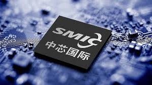
The extreme ultraviolet lithography machine (EUV), used to create circuitry patterns on silicon wafers, is possibly the most important chipmaking equipment banned in China. Used in the production of 7nm chips with the latest model helping foundries take their process nodes down to 2nm, China’s leading foundry, SMIC, still relies on using older technology such as deep ultraviolet lithography (DUV). Some DUV machines, including immersion DUVs, are banned in China because they contain some parts built in the U.S.
For years, there has been talk that China would get around the EUV ban by developing its own machine. Rumors that Huawei was filing for a patent on parts of a China-built EUV machine had circulated a few years ago, although nothing has surfaced. If we focus on what is available to SMIC right here and right now, the foundry is said to be testing the first domestically built DUV machine in China, assembled by Shanghai Yuliangsheng Technology Co., a company with ties to Huawei.
This could be China’s first step toward a homegrown EUV
Immersion lithography replaces this gap with a liquid, usually highly purified water, increasing the numerical aperture (NA) and allowing for the creation of more intricate circuitry patterns on the wafer. The latter is the foundation of a chip as chips are built in layers on top of a wafer.
The Yuliangsheng DUV uses parts mostly made in China, although some parts are imported. The company behind the machine is hoping to eventually build the machine using parts only obtained inside China, which would allow SMIC to obtain immersion DUV equipment without having to deal with U.S. sanctions. The new machine being tested by SMIC is similar to ASML’s Twinscan NXT:1950i, which was launched by the Dutch firm in 2008. It was designed for single exposures that could be used to produce 32nm chips.
The Yuliangsheng DUV could help SMIC produce 7nm and 5nm chips
While the Yuliangsheng DUV can create patterns in a single exposure that can be used to build a 28nm component, using multiple patterns, the immersion DUV could be used to manufacture chips using SMIC’s 7nm and 5nm nodes. However, using multiple patterns is more expensive and could lead to overlay errors, which occur when the different layers are misaligned. Pitch walking is another issue that leads to inconsistent spacing between features. In other words, using multiple patterns will not only lead to lower yields but will also raise the price of the component.
All of this means that the eventual goal for SMIC would be the ability of SMIC and other Chinese foundries to obtain a domestically produced High NA EUV. If that occurs, SMIC would be, in theory, able to build cutting-edge 2nm chips and compete against TSMC and Samsung Foundry.
Will China be able to play catch-up?
However, since then, Huawei has tried to improve its chips by designing internal changes to its silicon. But not much progress has been made, and for that to happen, China will need to develop its own lithography machines. SMIC is expected to start using the Yuliangsheng DUV for its 28nm production by 2027.


“Iconic Phones” is coming this Fall!
Good news everyone! Over the past year we’ve been working on an exciting passion project of ours and we’re thrilled to announce it will be ready to release in just a few short months.
LEARN MORE AND SIGN UP FOR EARLY BIRD DISCOUNTS HERE
#SMIC #testing #Chinesebuilt #immersion #lithograhy #machine

